— EDU — p-n junction under illumination
Attention
This tutorial is under construction
Header
- Files for the tutorial located in nextnano++\examples\education
p-n-junction-illuminated_GaAs_Nelson_2003_1D_nnp.in
- Main adjustable parameters in the input file:
parameter
$sun
- Relevant output files:
bias_XXXXX\bandedges.dat
bias_XXXXX\density_electon.dat
bias_XXXXX\density_hole.dat
bias_XXXXX\electric_field.dat
bias_XXXXX\potential.dat
IV_characteristics.dat
Introduction
In this tutorial, we introduce simulation of a solar cell with nextnano++. This tutorial is based on \(\S6\) in [NelsonPSC2003] and \(\S13\) in [Sze_Kwok_2007]. Solar cells work based on p-n junction, which is explained in detail in — NEW/EDU — p-n junction in the dark. Therefore, we recommend that you read it before going through this tutorial. In addition, GaAs solar cell will help you understand the simulation scheme for solar cells used in nextnano++.
How to illuminate in nextnano++
To control the concentration of the irradiated light, you have to adjust some variables in nextnano++.
$sun    = 10       # concentration of the sun, 10 is used for this tutorial

optics{
    irradiation{
        min_energy          = 0.01
        max_energy          = 5
        energy_resolution   = 1e-4

        global_illumination{
            direction_x = 1
            database_spectrum{
                name = "Solar-ASTM-G173-global"
                concentration = $sun
            }
        }
        global_reflectivity{
            database_spectrum{ name = "GaAs" }
        }
        global_absorption_coeff{
            database_spectrum{ name = "GaAs" }
        }
    }
}
min_energy and max_energy correspond to the minimum and maximum energy of irradiated photons.
energy_resolution is the energy step which is used to calculate optical properties.
$sun controls the concentration of the incident light as it can be defined at global_illumination{ database_spectrum{ concentration = $sun } }.
In this tutorial, Solar-ASTM-G173-global, which is equivalent to the solar spectrum, is also used as in GaAs solar cell.
The data of reflectivity and absorption coefficient of GaAs is written at database{ } at the end of the input file.
You can refer to GaAs solar cell for further information.
Short circuit
Let us investigate the behavior of p-n junction when it is illuminated by the sun light. First, we consider when the voltage across the diode is zero. We call the condition short circuit. The junction before the illumination is at equilibrium, having the space charge region and the electric field as shown in Figure 2.4.71 (a). The electric field impedes the diffusion of majority carriers as explained in — NEW/EDU — p-n junction in the dark.

Figure 2.4.71 The schematic images showing the principles of a solar cell. (a) is the p-n junction at equilibrium. When it is illuminated, an electron-hole pair is generated at the junction (b). The current runs as long as the diode is illuminated (c). We assume the resistance of the light bulb is zero because of the short circuit.
When the light is illuminated, it excites an electron in the valence band if the energy of the light is bigger than the band gap. The excited electron goes to the conduction band and becomes a conduction electron. On the other hand, a hole is generated at the valence band, instead of the excited electron. The electric field drifts the electron-hole pair and the electron goes to the n-doped GaAs whereas the hole goes to the p-doped GaAs as the result (Figure 2.4.71 (b)). As long as the junction is illuminated, the electron-hole pair is generated and constitutes the current (Figure 2.4.71 (c)).
Figure 2.4.72 shows the band profile and the carrier densities at short circuit. bandedges.dat, density_electon.dat, and density_hole.dat are used to produce this figure.

Figure 2.4.72 The band profiles are plotted in (a). When the light reaches the junction and the energy is bigger than the band gap, the electron-hole pair is generated as shown in (b). The carrier densities are plotted in (c). The hole density is shown in violet, whereas the electron density is in green.
In (a), \(\mathrm{CB}\) and \(\mathrm{VB}\) represent conduction and valence band, respectively. \(\mathrm{E}_{Fn}\) and \(\mathrm{E}_{Fp}\) are the electron quasi Fermi level and the hole quasi Fermi level. The results are in a good agreement with Fig. 6.8. in [NelsonPSC2003].
As you can see from Figure 2.4.72 (a) and (b), the built-in-potential \(V_{bi}\) is formed across the junction and the carriers generated by the illuminated light are drifted by the electric field. In addition, the quasi Fermi levels are split since the carriers are drifted and the carrier densities \(n\) and \(p\) increase above their equilibrium values.
In the short circuit, the photocurrent density \(J_{ph}\) is called the short-circuit current density \(J_{sc}\). The short-circuit current density is the maximum current density that the solar cell can produce.
The Photovoltatic effect
When the circuit is connected to a resistive load, the negative charges accumulated at n-doped GaAs and the positive charges accumulated at p-doped GaAs form a voltage (photovoltage). The current flows through the diode due to the voltage and is analogy to the current which flows across the diode under applied bias in the dark. Therefore, this current is called the dark current. The dark current density (\(J_{dark}\)) is in the opposite direction to the photocurrent density (\(J_{ph}\)) as shown in Figure 2.4.73.
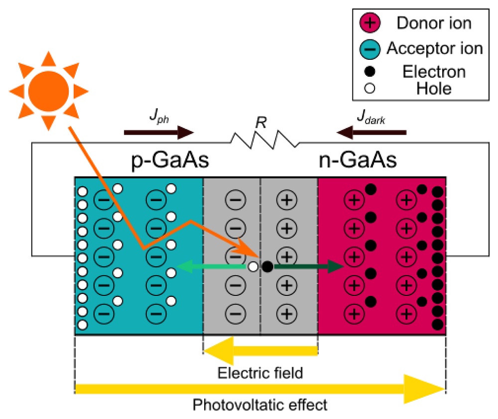
Figure 2.4.73 The circuit is connected to a resistive load. Note that \(J_{dark}\) flows in the opposite direction to \(J_{ph}\).
Generally speaking, when the photovoltage \(V\) is across the diode, the current density \(J\) through the diode can be expressed with the superposition approximation as below.
The photovoltage \(V\) is defied so that the forward bias is applied to the diode, where \(V > 0\). In the superposition approximation, the photocurrent density is independent of the applied voltage (\(J_{ph}(V) = J_{sc}\)). Note that we do not take into account the intensity of the irradiated light and the temperature of the diode here for the sake of simplicity. The effects will be explained in the last section of this tutorial.
\(J_{dark}(V)\) can be expressed by the equation described in — NEW/EDU — p-n junction in the dark.
where \(m\) is the ideality factor and \(J_{m,0}\) is a constant. The recombination current density \(J_{scr}\) is dominant and \(J_{m,0}\) becomes \(J_{scr,0}\) when \(m = 2\). On the other hand, the diffusion current density \(J_{diff}\) is much bigger than \(J_{scr}\) and \(J_{m,0}\) becomes \(J_{diff,0}\) when \(m = 1\).
As a result,
Now, let us look into the situation \(V = 0.5\;\mathrm(V)\). In nextnano++, we can set the situation by applying forward bias externally to the diode. Thus, the applied bias is equivalent to the photovoltage across the diode. Figure 2.4.74 shows the band profiles and the carrier densities of the diode under \(0.5\;\mathrm(V)\).
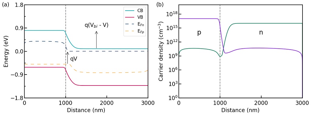
Figure 2.4.74 The band profiles are plotted in (a). The carrier densities are plotted in (b). The hole density is shown in violet, whereas the electron density is in green.
The results are very similar to Fig. 6.8. in [NelsonPSC2003]. As in the diode with forward bias, the built-in-potential is reduced to \(V_{bi} - V\). Applying the bias splits the quasi Fermi levels within the space charge region and the difference of the quasi Fermi levels is equivalent to \(qV\) as shown in Figure 2.4.74 (a).
Open circuit
When the circuit is open (open circuit), the photovoltage \(V\) across the diode is called the open-circuit voltage \(V_{oc}\).
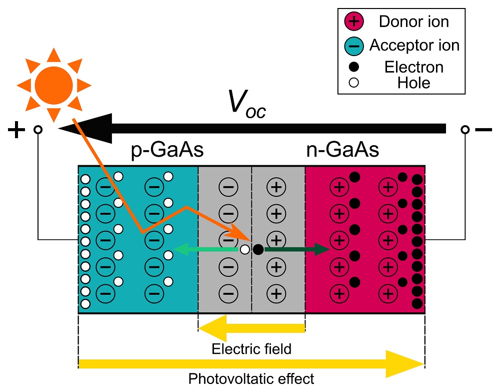
Figure 2.4.75 The circuit is open and the voltage \(V_{oc}\) is applied to the diode.
Since \(J(V) = 0\) in (2.4.17) in this case,
The open-circuit voltage is the maximum voltage that the solar cell can produce.
J-V curve
We look into the output characteristics of the solar cell in this section. Figure 2.4.76 shows J-V curves of the solar cell under the illumination and under the dark condition.
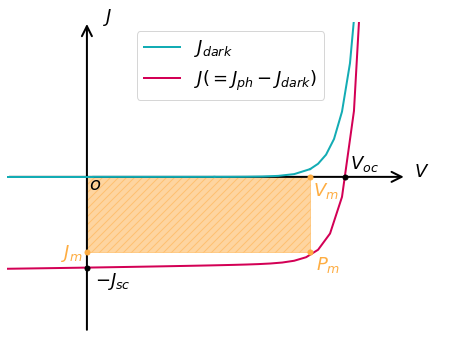
Figure 2.4.76 The J-V curves of the solar cell. The J-V curve under the illumination is shown in violet, whereas the J-V curve under the dark condition is in light-blue. The orange-filled area indicates the output of the maximum power density of the solar cell.
Again, the maximum current density that the solar cell can produce is the short-circuit current density, and the maximum voltage of the cell is the open-circuit voltage. However, the output of the maximum power density \(P_{m}\) is not equal to the product of them. It is represented by the intersection of \(J_{m}\) and \(V_{m}\).
This arises from the parasitic resistances which are connected in series and parallel to the solar cell. The series resistance consist of the electrical resistance present on the carrier transport path, such as the semiconductors and the contacts of the solar cell. The parallel resistance is attributed to leakage of the current due to defects in the solar cell.
We can derive \(P_{m}\) using the equations described in the sections above.
First, the power density of the solar cell is given by
The condition for the maximum power density is achieved when \(dP/dV = 0\).
Thus,
where \(\beta = q/k_{B}T\).
Therefore,
where \(FF\) is called the fill factor and the ratio to measure the sharpness of the J-V curve.
In addition, the energy conversion efficiency of the solar cell (\(\eta\)) is derived by dividing \(P_{m}\) by the incident power of the sun \(P_{in}\).
Effects of irradiation intensity and temperature
So far, the effects of the intensity of the incident light and temperature of the system on the behavior of the solar cell have not been considered. In this section, we briefy investigate the effects on J-V characteristics.
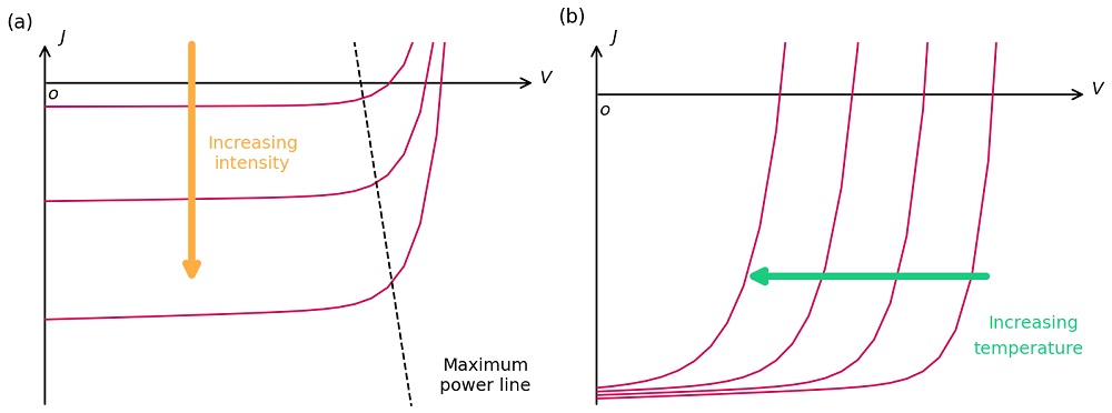
Figure 2.4.77 The J-V curves of the solar cell under incident light of various intensities is shown in (a). The J-V curves of the solar cell under different temperatures are shown in (b). The arrows indicate the direction of increasing intensity of the incident sunlight or the temperature.
Effect of irradiation intensity
Figure 2.4.77 (a) illustrates the effect of the light intensity on the J-V curve. Since the generation rate for electron-hole pairs is proportional to the light intensity, the photocurrent increases as the light intensity gets bigger. From (2.4.18), \(V_{oc}\) also increases logarithmically with the irradiation intensity. Thus, the more intensive light enables to obtain a bigger output of the maximum power density. However, increasing the light intensity is not always good as the light also raises the temperature and increases the series resistance of the solar cell, which degrade the cell performance.
Effect of temperature
The effect of the temperature on the J-V curve is shown in (b) in Figure 2.4.77. As the temperature is increased, the intrinsic carrier density \(n_{i}\) increases exponentially. When the diffusion current is dominant in the dark current across the solar cell, \(J_{0}\) becomes \(J_{diff,0}\). Thus, \(J_{diff,0}\) is also increased as \(n_{i}\) increased. According to (2.4.18), \(V_{oc}\) decreases logarithmically with increasing \(J_{diff,0}\) under a given \(J_{sc}\).
This occurs more noticeably than when the recombination current is dominant (\(J_{0} = J_{scr,0}\)) since \(J_{diff,0}\) is proportional to \(n_{i}^2\), whereas \(J_{scr,0}\) is proportional to \(n_{i}\). The detailed equations of \(J_{diff,0}\) and \(J_{scr,0}\) are in — NEW/EDU — p-n junction in the dark.
Actually, \(J_{sc}\) becomes larger since the band gap is reduced as the temperature increases and lower energy photons can be absorbed. However, the gain in \(J_{diff,0}\) is more significant than the gain in \(J_{sc}\), which eventually leads to the decrease of \(V_{oc}\). Therefore, increasing temperature reduces the performance of the solar cell.
Exercises
under construction
Last update: 16/07/2024